Overcome Complex PCB Challenge with Selective Soldering Technology
Selective soldering technology provides a solution for handling complex PCB designs, especially excelling in high-density and mixed-assembly circuit board manufacturing.
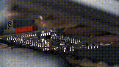
- Precise Positioning: Selective soldering allows operations on specific soldering points without affecting nearby sensitive components, such as SMD devices or non-soldering areas.
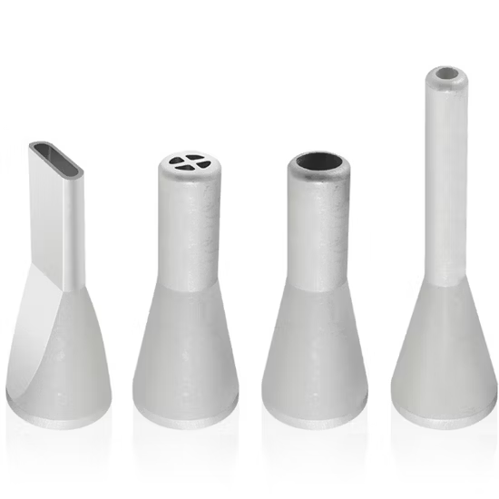
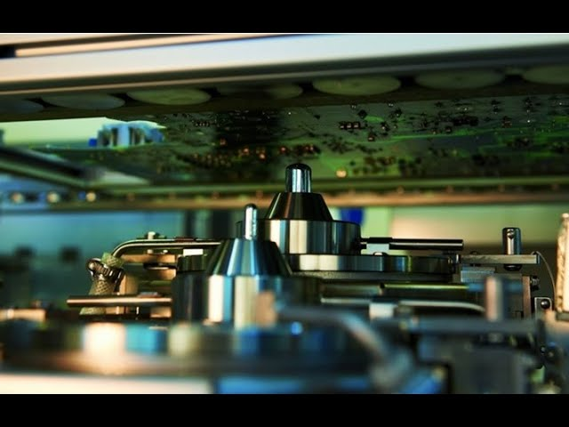
- Nozzle Technology: Using the Ersa VERSAFLOW as an example, its wetted circular nozzle design ensures that solder flows evenly in very tight spaces, effectively avoiding bridging issues while ensuring high-quality solder joint connections.
- Flexible Soldering: Supports both single-wave and multi-wave soldering modules to meet the production needs of PCBs with varying design complexities.
Fewer Defects And Higher Reliability with Selective Soldering Technology
Common soldering defects found in traditional wave soldering are significantly reduced with selective soldering.
- Precise Flux Application: Through micro-droplet application (such as the dual-nozzle configuration of the Ersa VERSAFLOW), flux is accurately applied to the solder joint area, preventing excess residue from contaminating non-soldering regions.
- Accurate Temperature Control: The preheating module can set temperature profiles according to PCB design requirements, minimizing component damage caused by temperature fluctuations. Additionally, the use of top heaters ensures better through-hole filling results.
- Anti-oxidation: The nitrogen atmosphere protects the solder from oxidation, thus improving the long-term stability and reliability of the solder joints.
Cost Savings in Material and Energy
Selective soldering technology optimizes material usage and production processes, leading to significant reductions in manufacturing costs.
- Less Solder Consumption: The miniaturized solder bath design (e.g., with a 10 kg capacity) helps avoid solder waste during dipping.
- Flux Reduction: Traditional atomization methods may lead to excessive flux, whereas selective soldering uses droplet spraying to precisely apply flux, reducing consumption and minimizing the need for cleaning processes.
- Efficient Energy Management: The modular, independent operation design shortens equipment cycle times, saving both space and energy costs.
Eco-Friendly: Reducing Solder Waste
As the manufacturing industry moves towards greener practices, selective soldering technology offers significant environmental benefits.
Eco-friendly Material: Supports lead-free soldering processes, reducing harmful chemical residues that impact the environment.
Some images are sourced online. Please contact us for removal if any copyright concerns arise.
Next: How Selective Soldering Meets the Demands of Industrial Control and Automotive Electronics
Custom Cables: Save 50%+ Avg Cost By JST, Molex, TE Alternatives | Processing Fee Down to $1 Per Piece | No Minimum Order Quantity (MOQ) Required
PCB & PCBA: New Customer Get Coupons Up to $125 | 1 – 32 Layers From $2 /5pcs | PCB Assembly From $8 /5pcs
Front Panels: High-quality Front Panel Acrylic/PET | Front Panel Order Up to 30% Off | Membrane Switch Available Soon