In modern electronic equipment, printed circuit boards (PCBs) bear the core function of electrical connection and signal transmission. The drilling process is an indispensable part of PCB manufacturing. Whether it is a micro motherboard for smartphones or a thick circuit board for industrial equipment, the quality of the drilled holes directly impacts signal integrity, device reliability, and machine performance. We will analyze the technical connotation and application scenarios of the PCB drilling process.
Purpose of PCB Drilling Process
The essence of PCB drilling is the formation of through-hole or blind-hole structures in insulating substrates (e.g., FR-4, high-frequency ceramics, etc.) and copper-clad laminates. These holes, through subsequent metallization, become conductive channels between different circuit layers or provide mounting space for the pins of electronic components. The following points summarize its core functions:
- Interlayer interconnection:
In multilayer PCBs, by drilling holes and plating them, it’s possible to connect the layers of copper foil to form a complete circuit network.
- Component mounting:
Using drilled holes helps realize electrical connections, and the holes also provide mounting locations for inline components or mechanical fixings.
- Heat dissipation and structural reinforcement:
Some of the holes also help dissipate heat and enhance the thermal management performance of the board.
Types of Holes
Holes on PCBs are categorized as plated through holes (PTH) and non-plated through holes (NPTH), depending on whether they participate in electrical connections.
Plated Through Holes (PTH)
PTH’s hole walls are formed with a conductive layer by chemical copper deposition and plating processes. Additionally, The walls are primarily for electrical interconnections or component mounting. The types of holes it covers include:
- Through-Hole Via: Throughout the PCB, connecting all layers.
- Blind Via: Extending from the surface to one of the inner layers without penetrating the entire board.
- Buried Via: Completely between the inner layers, without touching the surface.
Among them, through-hole vias are used for inserting component pins and interlayer signaling; blind vias are mainly used in high density boards (HDI) to connect the surface layer with the inner layer of the circuit; buried vias are used in the inner interconnections of complex multilayer boards to reduce the pressure on the surface layer wiring.
Non-Plated Through Holes (NPTH)
NPTHs have unmetallized hole walls, they are typically for the purpose of mechanical fixing or heat dissipation with no electrical function. Its common types include:
- Mechanical Mounting Holes: They are large in diameter and are for fixing PCBs or mounting heat sinks and enclosures.
- Positioning Holes: Used as an alignment reference during production or assembly to ensure inter-layer alignment accuracy.
- Heat Sink Holes: densely arranged underneath heat generating components to enhance heat dissipation efficiency.
- Special Function Holes: Some designs may contain unplated blind or buried holes for non-electrical applications (e.g. isolation structures).
Drilling Method and Process
Drilling Methods
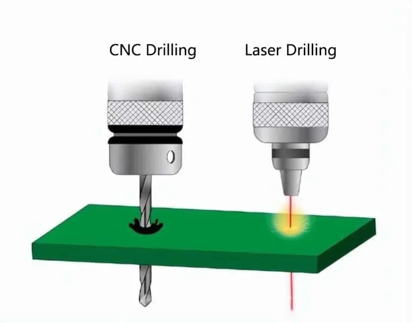
After decades of development in the PCB industry, using mechanical drills to create holes has consistently remained the mainstream technology. Mechanical drilling has withstood the growing demand for PCBs and it remains as a safe and cost-effective method for making holes. Certainly, for circuit boards with small aperture requirements, using laser drilling is also feasible, but the cost is much higher.
- Mechanical Drilling: A high-speed rotating drill (usually a carbide or diamond drill) is used to drill the PCB. This method is suitable for regular–sized holes with high productivity but may be limited for micro-holes due to drill bit wear.
- Laser Drilling: High-energy laser focusing generates localized high temperatures, causing the substrate to melt or vaporize, resulting in the formation of holes. Laser drilling is suitable for processing micro holes of very small sizes and high–density boards, but is more costly and requires more stringent optical properties of the material.
PCB Drilling Process
The entire drilling process usually consists of the following steps:
-
Pre-Preparation:
Inspection of PCB boards to determine board flatness, thickness, and pre-treatment; Generation of drilling files (e.g. Gerber files) according to the design drawings.
-
Precise Positioning:
Fix the PCB board on the drilling machine table and carry out precise positioning to ensure that the position, diameter, and depth of each hole meet the design requirements.
-
Drilling Operation:
Drill the holes according to the preset parameters (rotational speed, etc.) to ensure the hole wall is flat and burr-free.
-
Post-Processing:
This includes deburring, cleaning of residual debris in the holes, and subsequent processing, such as plating or copper cladding, to ensure the quality of the hole walls and the reliability of the electrical interconnections.
The PCB drilling process, from stacked board preparation to final inspection, involves the synergy of mechanical, chemical, optical, and other multidisciplinary technologies. Mechanical drilling is still the mainstream by virtue of the cost advantage, while laser drilling is gradually popularized in high–density boards (HDI).
The core of the process lies in precision control (hole diameter, position) and hole wall quality (smoothness, plating uniformity). The processes directly determine the electrical performance and reliability of the PCB. In the future, with the demand for high-density interconnections in 5G and AI chips, the drilling process will continue to break through to smaller hole diameters and higher depth-to-diameter ratios.
Some images are sourced online. Please contact us for removal if any copyright concerns arise.
Custom Cables: Save 50%+ Cost By JST, Molex, TE Alternatives | Processing Fee Down to $1/pcs | No Minimum Required
PCB & PCBA: New Customer Get Coupons Up to $125 | 1 – 32 Layers From $2/5pcs | PCB Assembly From $8/5pcs
Front Panels: High-quality Front Panel Acrylic/PET | Front Panel Order Up to 30% Off | Membrane Switch Available Soon